Original Link: https://www.anandtech.com/show/12785/arm-cortex-a76-cpu-unveiled-7nm-powerhouse
Arm's Cortex-A76 CPU Unveiled: Taking Aim at the Top for 7nm
by Andrei Frumusanu on May 31, 2018 3:01 PM EST- Posted in
- CPUs
- Arm
- Smartphones
- Mobile
- SoCs
- Cortex-A76

Another year, another TechDay from Arm. Over the last several years Arm’s event has come as clockwork in the May timeframe and has every time unveiled the newest flagship CPU and GPU IPs. This year is no exception as the event is back on the American side of the Atlantic in Austin Texas where Arm has one of its major design centres.
Two years ago during the unveiling of the Cortex A73 I had talked a bit more about Arm’s CPU design teams and how they’re spread across locations and product lines. The main design centres for Cortex-A series of CPUs are found in Austin, Texas; Cambridge, the United Kingdom, and Sophia-Antipolis in the south of France near Nice. For the last two years the Cortex A73 and Cortex A75 were designs that mainly came out of the Sophia team while the Cortex A53 and more recently the A55 were designs coming out of Cambridge. This means that we haven’t seen any recent designs coming out of Austin and the last of the “Austin family” of CPUs were the A57 and A72.
The project being worked on in Austin had been hyped up for several years – I remember even as early as the A73 release back in 2016 the company had pulled forward some elements from an advanced future microarchitecture on the back-end pipelines, especially on the FP/SIMD side. The Cortex A75 was further remarked as pulling more elements from this new mysterious project.
Today we can finally unveil what the Austin team has been working on – and it’s a big one. The new Cortex A76 is a brand new microarchitecture which has been built from scratch and lays the foundation for at least two more generations for what I’ll call “the second generation of Austin family” of CPUs.
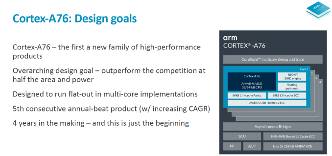
The Cortex A76 is important for Arm for a design perspective as it represents a new start from a clean sheet. It’s rare for IP claim to be able to do this as it represents a great resource and time investment and if it weren’t for the Sophia design team taking over the steering wheel for the last two generations of products it wouldn’t have been reasonable to execute. The execution of the CPU design teams should be emphasised in particular as Arm claims this is the 5th generation “annual beat” product where the company delivers a new microarchitecture every new year. Think of it as an analogue to Intel’s past Tick-Tock strategy, but rather Tock-Tock-Tock for Arm with steady CAGR (compound annual growth rate) of 20-25% every generation coming from µarch improvements.
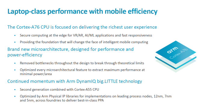
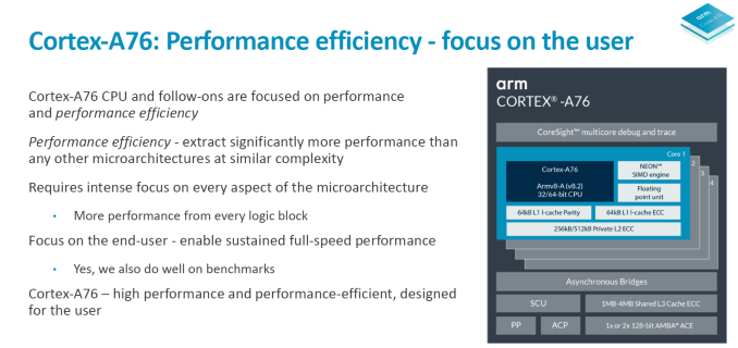
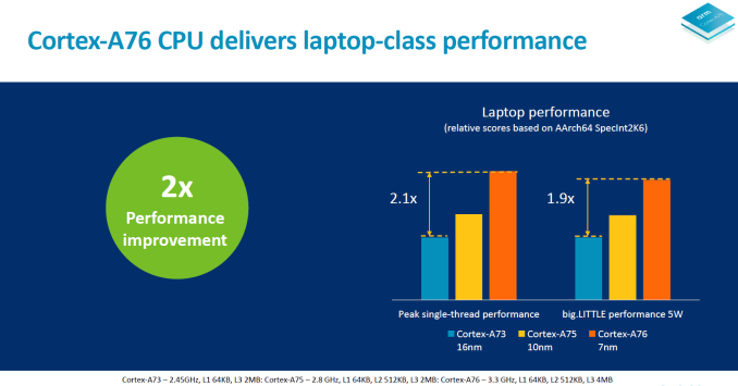
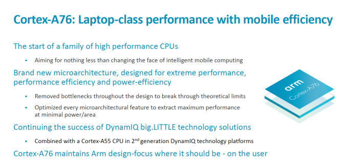
So what is the Cortex A76? In Arm’s words, it’s a “laptop-class” performance processor with mobile efficiency. The vision of the A76 as a laptop-class processor had been emphasised throughout the TechDay presentation so it seems Arm is really taking advantage of the large performance boost of the IP to cater to new market segments such as the emerging “Always connected PCs” which Qualcomm is spearheading with their SoC platforms.
The Cortex A76 microarchitecture has been designed with high performance while maintaining power efficiency in mind. Starting from a clean sheet allowed the designers to remove bottlenecks throughout the design and to break previous microarchitectural limitations. The focus here was again maximum performance while remaining within energy efficiency that is fit for smartphones.
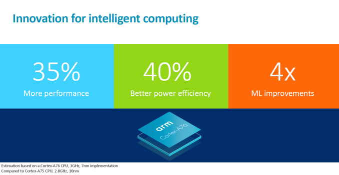
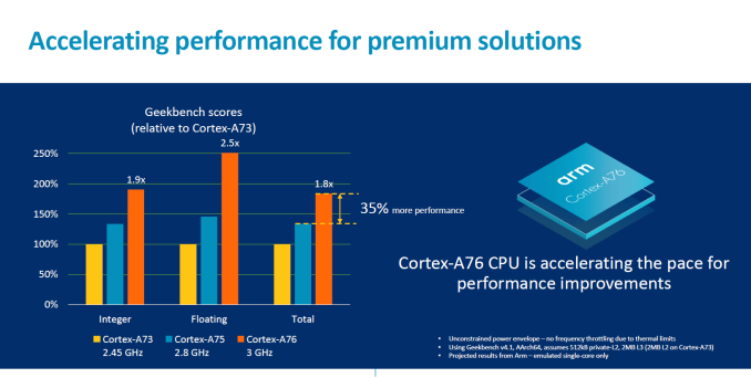
In broad metrics, what we’re promised in actual products using the A76 is the follows: a 35% performance increase alongside 40% improved power efficiency. We’ll also see a 4x improvements in machine learning workloads thanks to new optimisations in the ASIMD pipelines and how dot products are handled. These figures are baselined on A75 configurations running at 2.8GHz on 10nm processes while the A76 is projected by Arm to come in at 3GHz on 7nm TSMC based products.
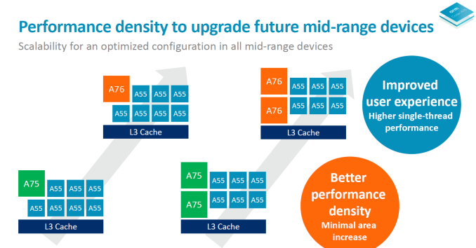
The new CPU is naturally still compatible with DynamIQ’s common cluster topology and Arm envisions designs to be paired with Cortex A55s as the little more power efficient CPUs. The configuration scalability of the DynamIQ IP again was reiterated and we were presented with example configurations such as 1+7 or 2+6 with either Cortex A75 or A76 CPU IP. This presentation slide was one of the rare ones where Arm referred to the area size of the A76, pointing out that the A75 still had better PPA and thus might still be a valid design choice for companies, depending on their needs. One comparison that was made during the event is that in terms of area, three A76’s with larger caches would fit inside the size of a Skylake core – all while within 10% of the IPC of the Intel CPU, but obviously there’s also process node scaling considerations to take into account.
A standout claim is that Arm aims to outperform the competition at half the area and half the power. Arm was slightly beating around the bush here in what it considers the competition, but generally the answer was that it was considering everybody the competition. Taking into account Intel, AMD or Samsung it’s actually not that hard to imagine Arm beating them in PPA as historically the company always had the smallest CPU designs and that directly translates into more efficient microarchitectures.
Before we get into more detailed breakdowns of the performance and power improvements and what I’m expecting to happen into products, let’s see the microarchitectural improvements on the core and how Arm managed to extract this much performance while maintaining power efficiency.
Cortex A76 µarch - Frontend
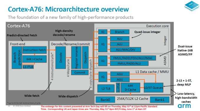
Starting off with a rough overview of the Cortex A76 microarchitectural diagram we see the larger functional blocks. The A76 doesn’t look too different than other Arm processors in this regard and the differences come only with details that Arm is willing to divulge. To overly simplify it, this is a superscalar out-of-order core with a 4-wide decode front-end with 8 execution ports in the backend with a total implementation pipeline depth of 13 stages with the execution latencies of a 11 stage core.
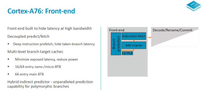
In the front-end, Arm has created a new predict/fetch unit that it calls a “predict-directed fetch”, meaning the branch prediction unit feeds into the instruction fetch unit. This is a divergence from past Arm µarches and it allows for both higher performance and lower power consumption.
The branch prediction unit is what Arm calls a first in the industry in adopting a hybrid indirect predictor. The predictor is decoupled from the fetch unit and its supporting large structures operate separate from the rest of the machine – likely what this means is that it will be easier to clock-gate during operation to save on power. The branch predictor is supported by 3-level branch target caches; a 16-entry nanoBTB, a 64-entry microBTB and a 6000 entry main BTB. Arm claimed back in the A73 and A75 generations of branch predictors were able to nearly predict all taken branches so this new unit in the A76 seems to be one level above that in capability.
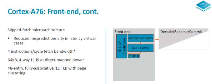
The branch unit operates at double the bandwidth of the fetch unit – it operates on 32B/cycle meaning up to 8 32b instructions per cycle. This feeds a fetch queue in front of the instruction fetch consisting of 12 “blocks”. The fetch unit operates at 16B/cycle meaning 4 32b instructions. The branch unit operating at double the throughput makes it possible to get ahead of the fetch unit. What this serves is that in the case of a mispredict it can hide branch bubbles in the pipeline and avoid stalling the fetch unit and the rest of the core. The core is said to able to cope with up to 8 misses on the I-side.
I mentioned at the beginning that the A76 is a 13-stage implementation with the latency of an 11-stage core. What happens is that in latency-critical paths the stages can be overlapped. One such cycle happens between the second cycle of the branch predict path and the first cycle of the fetch path. So effectively while there’s 4 (2+2) pipeline stages on the branch and fetch, the core has latencies of down to 3 cycles.
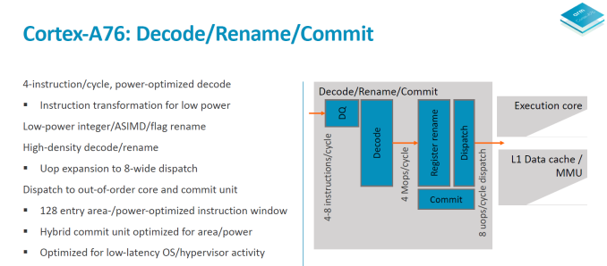
On the decode and rename stages we see a throughput of 4 instructions per cycle. The A73 and A75 were respectively 2 and 3-wide in their decode stages so the A76 is 33% wider than the last generation in this aspect. It was curious to see the A73 go down in decode width from the 3-wide A72, but this was done to optimise for power efficiency and “leanness” of the pipeline with goals of improving the utilisation of the front-end units. With the A76 going 4-wide, this is also Arms to date widest microarchitecture – although it’s still extremely lean when putting it into juxtaposition with competing µarches from Samsung or Apple.
The fetch unit feeds a decode queue of up to 16 32b instructions. The pipeline stages here consist of 2 cycles of instruction align and decode. It looks here Arm decided to go back to a 2-cycle decode as opposed to the 1-cycle unit found on the A73 and A75. As a reminder the Sophia cores still required a secondary cycle on the decode stage when handling instructions utilising the ASIMD/FP pipelines so Arm may have found other optimisation methods with the A76 µarch that warranted this design decision.
The decode stage takes in 4 instructions per cycle and outputs macro-ops at an average ratio of 1.06Mops per instruction. Entering the register rename stage we see heavy power optimisation as the rename units are separated and clock gated for integer/ASIMD/flag operations. The rename and dispatch are a 1 cycle stage which is a reduction from the 2-cycle rename/dispatch from the A73 and A75. Macro-ops are expanded into micro-ops at a ratio of 1.2µop per instruction and we see up to 8µops dispatched per cycle, which is an increase from the advertised 6µops/cycle on the A75 and 4µops/cycle on the A73.
The out-of-order window commit size of the A76 is 128 and the buffer is separated into two structures responsible for instruction management and register reclaim, called a hybrid commit system. Arm here made it clear that it wasn’t focusing on increasing this aspect of the design as it found it as a terrible return on investment when it comes to performance. It is said that the performance scaling is 1/7th – meaning a 7% increase of the reorder buffer only results in a 1% increase in performance. This comes at great juxtaposition compared to for example Samsung's M3 cores with a very large 224 ROB.
As a last note on the front-end, Arm said to have tried to optimised the front-end for lowest possible latency for hypervisor activity and system calls, but didn’t go into more details.
Cortex A76 µarch - Backend
Switching to the back-end of the core we have a look at the execution core.
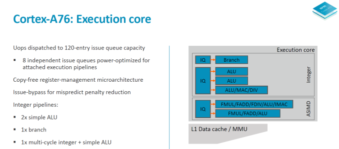
The integer core contains 6 issue queues and execution ports (4 depicted in the slide plus 2 load/store pipelines). There are 3 integer execution pipelines – two ALUs capable of simple arithmetic operations and a complex pipeline handling also multiplication, division and CRC ops. The three integer pipelines are served by 16 deep issue queues. The same size issue queue can also be found serving the single branch execution port.
Two load/store units are the remaining ports of the integer core and are each served by two 12 deep issue queues. The issue queue stages are 3 cycles deep and while I mentioned that the rename/dispatch is 1 stage deep, the dispatch stage actually overlaps with the first cycle of the issue queues stages.
The ASIMD/floating point core contains two pipelines which are served by two 16-deep issue queues.
When it comes to the backend of a CPU core the two most important metrics are instruction throughput and latency. Where the A76 in particular improves a lot is in terms of instruction latency as it’s able to shave off cycles on very important instructions.
To better overview the improvements I created a table with the most common instruction types. The execution throughput and latencies presented here are for AArch64 instructions and if not otherwise noted represent operations on 64-bit data for integer and 64bit (double precision) FP.
| Backend Execution Throughput and Latency | ||||||
| Cortex-A75 | Cortex-A76 | Exynos-M3 | ||||
| Exec | Lat | Exec | Lat | Exec | Lat | |
| Integer Arithmetic (Add, sub) | 2 | 1 | 3 | 1 | 4 | 1 |
| Integer Multiply 32b | 1 | 3 | 1 | 2 | 2 | 3 |
| Integer Multiply 64b | 1 | 3 | 1 | 2 | 1 (2x 0.5) |
4 |
| Integer Multiply Accumulate | 1 | 3 | 1 | 2 | 1 | 3 |
| Integer Division 32b | 0.25 | 12 | 0.2 | < 12 | 1/12 - 1 | < 12 |
| Integer Division 64b | 0.25 | 12 | 0.2 | < 12 | 1/21 - 1 | < 21 |
| Move (Mov) | 2 | 1 | 3 | 1 | 3 | 1 |
| Shift ops (Lsl) | 2 | 1 | 3 | 1 | 3 | 1 |
| Load instructions | 2 | 4 | 2 | 4 | 2 | 4 |
| Store instructions | 2 | 1 | 2 | 1 | 1 | 1 |
| FP Arithmetic | 2 | 3 | 2 | 2 | 3 | 2 |
| FP Multiply | 2 | 3 | 2 | 3 | 3 | 4 |
| FP Multiply Accumulate | 2 | 5 | 2 | 4 | 3 | 4 |
| FP Division (S-form) | 0.2-0.33 | 6-10 | 0.66 | 7 | >0.16 (2x 1+/12) |
12 |
| FP Load | 2 | 5 | 2 | 5 | 2 | 5 |
| FP Store | 2 | 1-N | 2 | 2 | 2 | 1 |
| ASIMD Arithmetic | 2 | 3 | 2 | 2 | 3 | 1 |
| ASIMD Multiply | 1 | 4 | 1 | 4 | 1 | 3 |
| ASIMD Multiply Accumulate | 1 | 4 | 1 | 4 | 1 | 3 |
| ASIMD FP Arithmetic | 2 | 3 | 2 | 2 | 3 | 2 |
| ASIMD FP Multiply | 2 | 3 | 2 | 3 | 1 | 3 |
| ASIMD FP Chained MAC (VMLA) | 2 | 6 | 2 | 5 | 3 | 5 |
| ASIMD FP Fused MAC (VFMA) | 2 | 5 | 2 | 4 | 3 | 4 |
On the integer operations side the A76 improves the multiplication and multiply accumulate latencies from 3 cycles down to 2 cycles, with the throughput remaining the same when compared to the A75. Obviously because the A76 has 3 integer pipelines simple arithmetic operations see a 50% increase in throughput versus the A75’s 2 pipelines.
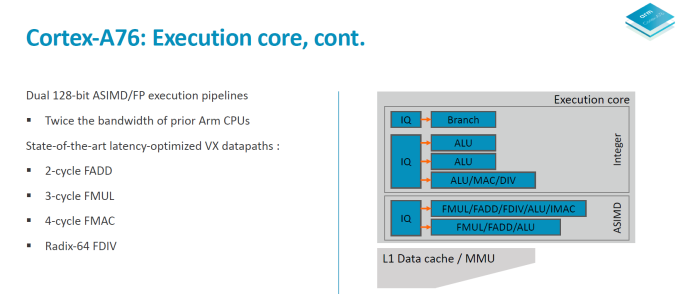
The much larger and important improvements can be found in the “VX” (vector execution) pipelines which are in charge of FP and ASIMD operations. Arm calls the new pipeline a “state-of-the-art” design and this is finally the result that’s been hyped up for several years now.
Floating point arithmetic operations have been reduced in latency from 3 cycles down to 2 cycles, and multiply accumulate has also shaved off a cycle from 5 cycles down to 4.
What Arm means by the “Dual 128bit ASIMD” with doubled execution bandwidth is that for the A75 and prior only one of the vector pipelines was capable of 128bit while the other one was still 64-bit. For the A76 both vector pipelines are 128-bit now so quad-precision operations see a doubling of the execution throughput.
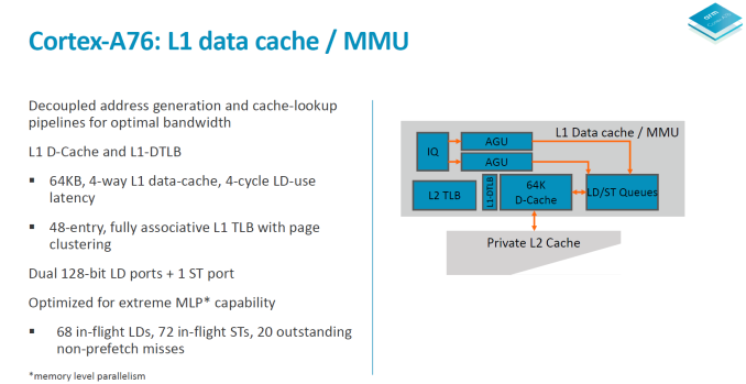
Moving onto more details of the data handling side, we see the again the two load/store pipelines which was something first implemented on the A73 and A75. Although depicted as one issue queue in the slide, the LD/S pipelines each have their own queues at 16 entries deep.
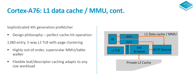
The data cache is fixed at 64KB and is 4-way associative. Load latency remains at 4 cycles. The DTLBs run a separate pipeline as tag and data lookup. Arm’s goals here is aiming for maximum MLP/ memory level parallelism to be able to feed the core.
In a perfect machine everything would be already located in the caches, so it’s important to have very robust prefetching capabilities. On the A76 we see a new 4th generation prefetchers introduced to get nearer to this goal of perfect cache-hit operation. In all the A76 has 4 different prefetching engines running in parallel looking at various data patterns and loading data into the caches.
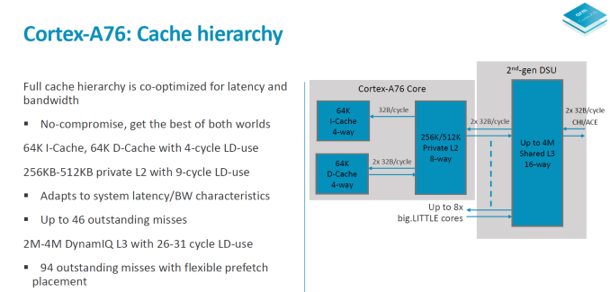
In terms of the A76 cache hierarchy Arm is said to have made no compromises and got the best of both worlds in terms of bandwidth and latency. The 64KB L1 instruction cache reads up to 32B/cycle and the same bandwidth applies to the L1 data cache in both directions. The L1 is a writeback cache. The L2 cache is configurable in 256 or 512KB sizes and is D-side inclusive with the same 2x 32B/cycle write and read interfaces up to the exclusive L3 cache in the 2nd generation DSU.
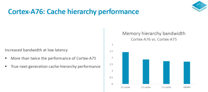
Overall the microarchitectural improvements on the core are said to improve memory bandwidth to DRAM by up to 90% in microbenchmarks.
All in all the microarchitecture of the A76 could be summed up in a few focus design points: Maximise memory performance throughout the core by looking at every single cycle. During the design phase the engineers were looking at feature changes with a sensitivity of up to 0.25% in performance or power – if that metric was fulfilled then it was deemed to be a worthwhile change in the core. Small percentages then in turn add up to create significant figures in the end product.
The focus on bandwidth on latency is said to have been extreme, and Arm was very adamant in re-iterating that to be able to take full advantage of the microarchitecture that vendors need to implement an equally capable memory subsystem on the SoC to see full advantages. A figure that was put out there was 0.25% of performance per nanosecond of latency to main memory. As we’ve seen in the Snapdragon 845 one of the reasons the SoC didn’t quite reach Arm’s projected performance metrics was the degraded memory latency figures which might have been introduced by the L4 system cache in the SoC. In the future vendors will need to focus more on providing latency sensitive memory subsystems as otherwise they’ll be letting free performance and power on the table with differences that could amount to basically a generational difference in CPU IP.
Performance & Power Projections
Now that we’ve had more insight into the A76’s microarchitecture – there’s always a disconnect between theoretical performance based on overlying µarch and how it ends up in practice. We’re first going to look at ISO-process and ISO-frequency comparisons which means the generational performance improvements between the cores with otherwise identical factors such as memory subsystems.
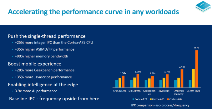
In terms of general IPC Arm promises a ~25% increase in integer workloads and a ~35% increase in ASIMD/floating point workloads. Together with up to 90% higher memory bandwidth figures compared to the A75 the A76 is then meant to provide around a 28% increase in GeekBench4 and 35% more JavaScript performance (Octane, JetStream). In AI inferencing workloads the doubled ASIMD 128-bit capabilities of the A76 serves to quadruple the general matrix multiply performance in half precision formats.
These performance figures are respectable but not quite earth-shattering considering the tone of the improvements of the µarch. However it’s to note that we’re expecting the A76 to come first be deployed in flagship SoCs on TSMC’s 7nm process which allows for increased clocks.
Here Arm’s projections is that we’ll be seeing the A76 clocked at up to 3GHz on 7nm, which in turn will result in higher improvements. Quoted figures are 1.9x in integer and 2.5x in floating point subscores of GeekBench4 while we should be expecting total score increases of 35%.
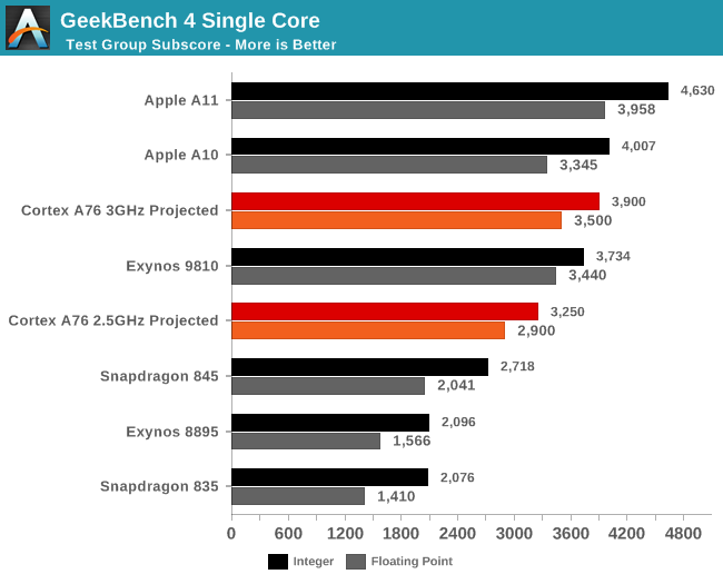
What this means in terms of absolute numbers is projected in the above graph. Baselining on the performance of the Snapdragon 835 and Snapdragon 845 a future SoC with an A76, 512KB L2’s and 2MB L3 would fall in around the GeekBench4 performance of the Exynos 9810 depending if the target 3GHz is reached.
In the past Arm has been overly optimistic when releasing frequency targets – for example the A73 was first projected at up to 2.8GHz and the Cortex A75 projected at up to 3GHz. In the end both ended up at no higher than 2.45GHz and 2.8GHz.
I’ve talked to a vendor about this and it seems Arm doesn’t take into consideration all corners when doing timing signoff, and in particular vendors have to take into consideration process variations which result in differently binned units, some of which might not reach the target frequencies. As mobile chips generally aren’t performance binned but rather power binned, vendors need to lower the target clock to get sufficient volume for commercialisation which results in slightly reduced clocks compared to what Arm usually talks about.
For the first A76 implementations in mobile devices I’m adamant that we won’t be seeing 3GHz SKUs but rather frequencies around 2.5GHz. Arm is still confident that we’ll see 3GHz SoCs but I’m going to be rather on the conservative side and be talking about 2.5GHz and 3GHz projections alongside each other, with the latter more of a projection of future higher TDP platforms.
Arm also had a slide demonstrating absolute peak performance at frequencies of 3.3GHz. The important thing to note here was that this scenario exceeded 5W and the performance would be reduced to get under that TDP target. It wasn’t clear if this was SoC power or solely CPU power – I’ll follow up with a clarification after I reach out to Arm.
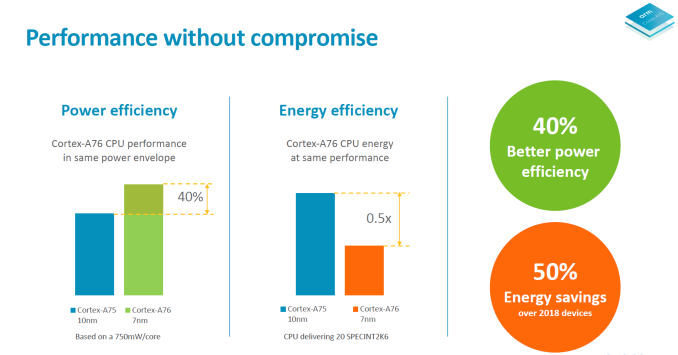
Obviously the most important metric here alongside the performance improvements is the power and efficiency targets. In target products comparing Cortex A75 on a 10nm process versus a Cortex A76 on a 7nm process under the same 750mW/core power budget, the Cortex A76 delivers 40% more performance.
In terms of energy efficiency, a 7nm A76 at a performance target of 20 SPECint2006 of an A75 on 10nm (meaning maximum performance at 2.8GHz) is said to use half the amount of energy.
What is important in all these metrics again is that we weren’t presented an ISO-process comparison or a comparison at maximum performance of the A76 at 3GHz, so we’re left with quite a bit of guesswork in terms of projecting the end energy efficiency difference in products. TSMC promises a 40% drop in power versus 10FF. We haven’t seen an A75 implemented on a TSMC process to date so the best baseline we have is Qualcomm’s Snapdragon 845 on Samsung 10LPP which should slightly outperform 10FF.
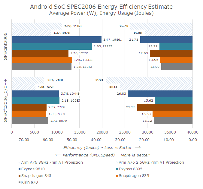
Going through my projected data on one side we have performance on the right side: I baselined the SPECspeed scores on the average of the Snapdragon 835 and Kirin 970 measured results and applied Arm’s projected IPC claims and scaled the scores for frequency. For the 3GHz A76 projection this gets us the near 2x performance improvements in SPECint2006 vs the A73 generation of cores.
In terms of power efficiency, there’s more guesswork as the only real figure we have is as earlier stated the process scaled efficiency figures. Arm quoted a performance target of 20 SPECint2006 which I suspect is a 2.8GHz A75 run with GCC compiled benchmark binaries which have an advantage over my LLVM figures. If Arm wanted to compare against the Snapdragon 845 this matches roughly a 2.4GHz A76. Accounting for the process power improvement this roughly leaves a ~15% microarchitectural advantage for the A76. However as the A76 is targeted to perform 35% higher, and as we’ve seen in the past performance increases through clock don’t scale linearly with power, the power and efficiency advantages would very quickly degrade at peak performance.
Taking all factor into account as best as I could, we should be seeing 7nm A76 based SoCs beat slightly beat the energy efficiency of current Arm SoCs in terms of absolute energy usage at peak performance, a metric which is important as it is directly proportional to a device’s battery life. At a more conservative 2.5GHz clock this energy efficiency advantage would be greater and around 30% less energy than current generation A73 and A75 SoCs.
So on one hand the A76 would be extremely energy efficient, but also it could very well be a thermally constrained design as its peak performance we’d be seeing quite higher TDP figures. Arm states that the A76 is meant to run at full frequency in quad-core mode, however that claim is limited to larger form-factors, as for mobile devices, based on what I’m hearing vendors, will need to tone it down to lower clocks in order to fit smartphone designs.
Again the projection here contain a lot of variables and I’m erring towards the more conservative side in terms of performance and efficiency- however it’s clear that the jump will be significant in whichever way vendors will decide to push the A76 in (Performance or efficiency).
Conclusion & Thoughts
The Cortex A76 presents itself a solid generational improvement for Arm. We’ve been waiting on a larger CPU microarchitecture for several years now, and while the A76 isn’t quite a performance monster to compete with Apple’s cores, it shows how important it is to have a balanced microarchitecture. This year all eyes were on Samsung and the M3 core, and unfortunately the performance increase came at a great cost of power and efficiency which ended up making the end-product rather uncompetitive. The A76 drives performance up but on every step of the way it still deeply focused on power efficiency which means we’ll get to see the best of both worlds in end products.
In general Arm promises a 35% performance improvement which is a significant generational uplift. Together with the fact that the A76 is targeted to be employed in 7nm designs is also a boost to the projected product.
I’m having some reservations in terms of the performance targets and if vendors will indeed release the SoC with quad-core clock rates of up to 3GHz – based on what I’ve heard from vendors that seems like a rather very optimistic target. Even then, a reduced clock frequency still brings significant benefits, and it’s especially on the efficiency side where Arm should be lauded for continuing to place great focus on.
Whether my projections are correct or not is something we’ll have to see in actual products, but fact is that we *will* see significant efficiency benefits in the next generation of SoCs which should bring both an notable performance improvement as well as battery life improvement to the user. Arm’s focus here on the user experience seems to be exemplary and I hope vendors will be able to implement the core based on Arm’s guidance and reach the targeted metrics.
The Cortex A76 is said to have already come back in working silicon at two partners and we’ll very likely see it shipping in commercial products by the end of the year. I won’t be beating around the bush here as Huawei and HiSilicon’s product cycle schedule makes it obvious that they’re likely one of the launch partners for the product. Qualcomm has also doubled down on using Arm cores in the mobile space so we should also be seeing the next generation Snapdragon SoCs employ the A76. Among the big players, it’s Samsung LSI which is going to have a tough time – the A76 doesn’t seem to greatly outperform the M3, so at least in theory, the M4’s focus will need to be solely on power efficiency. Then again Arm is very open about their design goals; half the area and half the power at similar performance is something that’s going to be hard to compete against.
The Cortex A76 is said to be the baseline microarchitecture on which Arm will iterate over the next 2 generations at least. Arm has been able to execute their yearly beat roadmap on time for 5 generations now and with yearly 20-25% CAGR it’s going to be a very interesting next couple of years as the mobile space is very quickly approaching the performance of desktop CPUs.

